
In today’s blog post, I am going to look at how to modify a chip found in a variety of vintage gear containing firmware. It is quite common for older gear to receive firmware upgrades stored on chips. I have a slightly older model chip and want to upgrade the firmware of my device.
To begin, I picked up an XGecu T48 programmer from Ali Express for £30 during the March ‘beginning of the month’ sale and some chips. Next I downloaded software for the T48 programmer (link), for Windows. Since I use a Mac, I installed VirtualBox and Windows 10. To get access to USB 2 speed from inside Virtual Box, I need to install the 6.1.x extenision pack (link) otherwise, only USB 1.1 will be active.
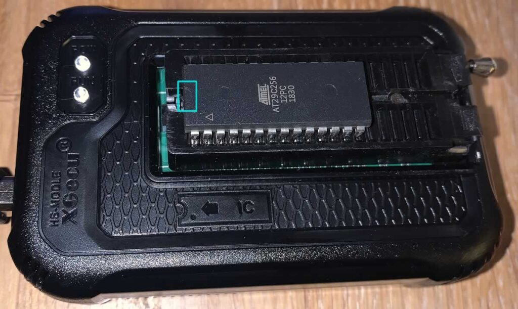
Next, I looked for the notch (pin 1) on the chip to identify which way round it goes. The notch points away from the lever, and points towards the blue light/usb port.
I plugged it all in. Since this was my first time running a T48, I was asked to reflash the T48 programmer firmware which was a bit of a surprise. This was completed by Tools -> Reflash Firmware. All went well and the flash completed successfully. The USB driver changed language to English which could be seen from the VirtualBox dropdown options list found under Device->USB. My T48 programmer was recognised correctly when plugged back in and worked fine.
To recognise the chip, I selected Search IC(S) and chose Search and Select.
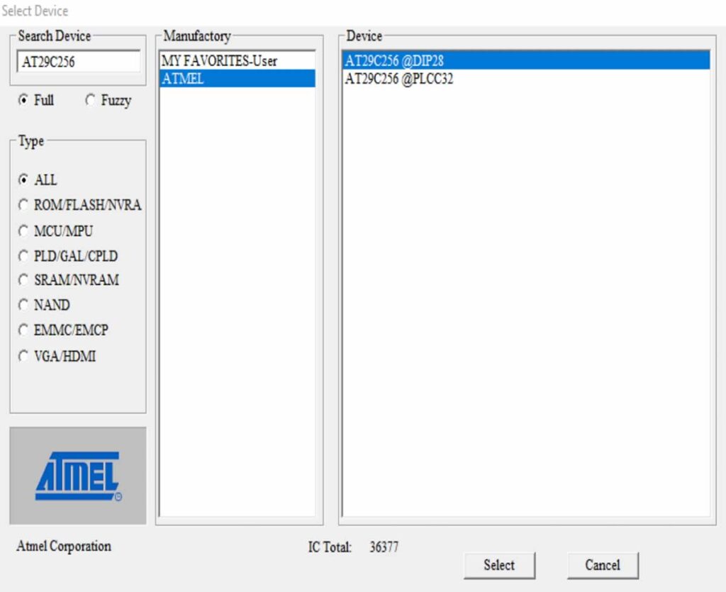
In the top left Search Device list, I typed in the AT29C256 chip and selected DIP 28. I bought the following chips:
- 1pcs/lot AT29C256-12PC AT29C256-15PC AT29C256-70PI AT29C256-90PI AT29C256 DIP-28 In Stock
- 5pcs/lot M2764A-10F1 M2764A-2F6 M2764A-2F1 25F1 3F1 M2764 = MBM2764 CDIP-28 In Stock
I selected the Atmel AT29C256 because it is a flash chip, perfect for learning, making mistakes, erasing and trying again. It is very forgiving. It is bigger than the recommended 8KB chip but my thoughts were, I just need to flash the image multiple times in steps of 8kB. My chip is 32kb in size. 0x00008000 = 32 KB. So, if I have a ROM image of 8KB, (32/8 = 4), I need to flash in 4 locations. 0000 0000, 0000 2000, 0000 4000, 0000 6000
I clicked on load, found the bin file and clicked select.
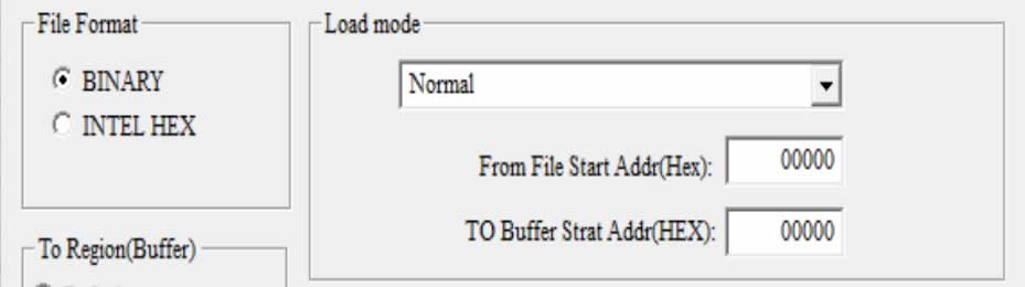
To start, I wrote to 00000. Perfect. Next, I then wrote to buffer location 02000 but crucially, disabled the buffer. This means, 0kB write, 8kB. I repeated or 04000 (16kB write) and 0600 24kB write. This means the same code has been written in four different locations and can be accessed by all of the pins across the chip.
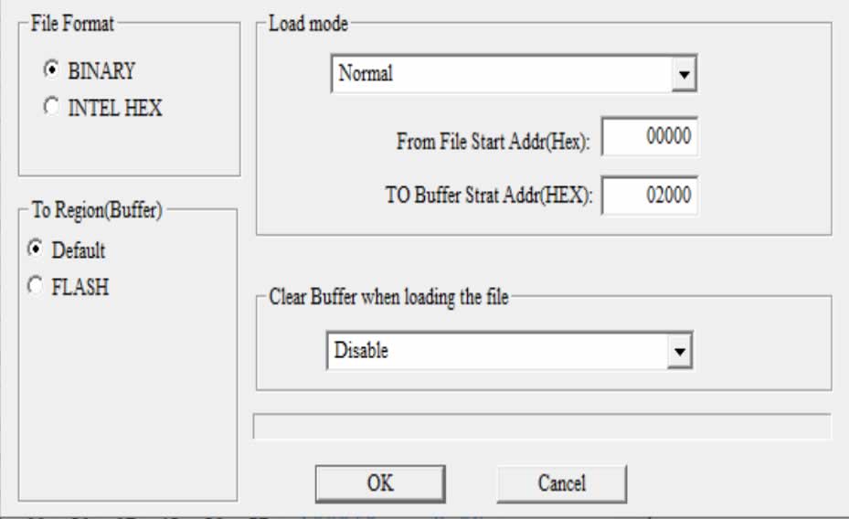
After reading through flashing notes, I reconsidered my decision and made an adjustment. Not sure if this is necessary but I double backed and also wrote to 0100, 0300, 0500 and 0700 to fill the entire space. These locations are blank anyway. It gave me a total of 8 locations with the same data in case data needed to be accessed in a different way than I thought, from different pins.
Finally, click on program.
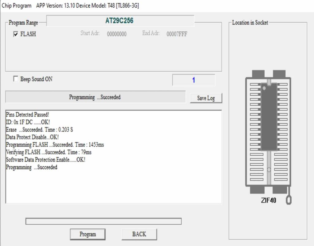
Okay, done and ready to go!
Next step involves plucking the chip out of my device and putting in the new firmware chip.